Here is an exclusive look at semiconductor material and device characterization solution manual. This comprehensive guide covers the essential aspects and latest developments within the field.

semiconductor material and device characterization solution manual continues to evolve as a critical topic in modern discourse. Our automated engine has curated the most relevant insights to provide you with a high-level overview.
"semiconductor material and device characterization solution manual is universally considered a compelling subject worthy of deeper analysis."
Below you will find a curated collection of visual insights and related media gathered for semiconductor material and device characterization solution manual.
Visual Gallery
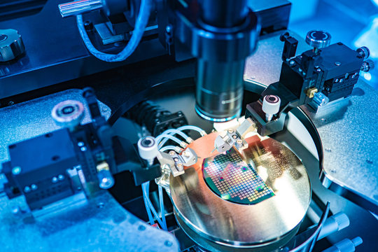
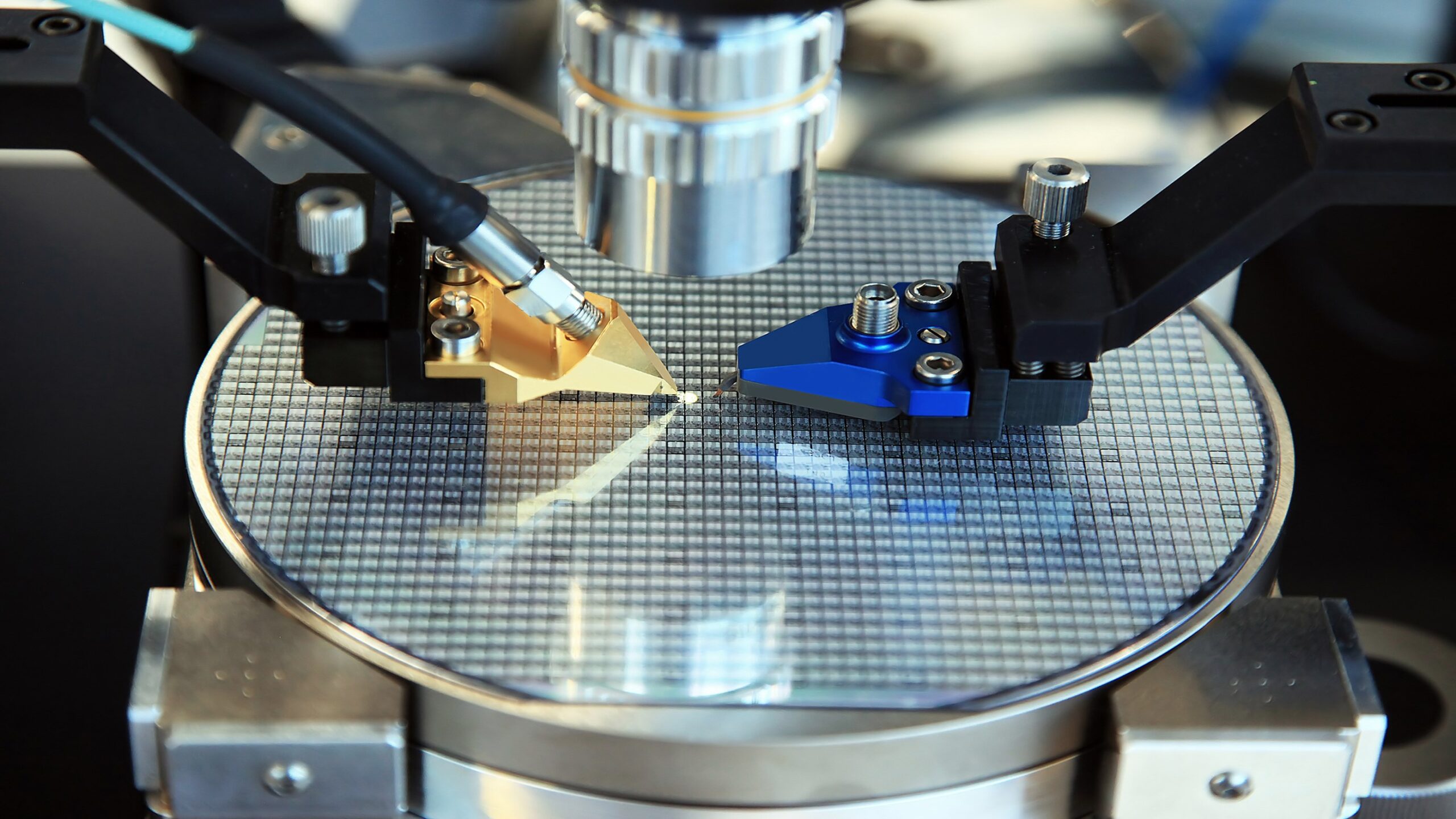
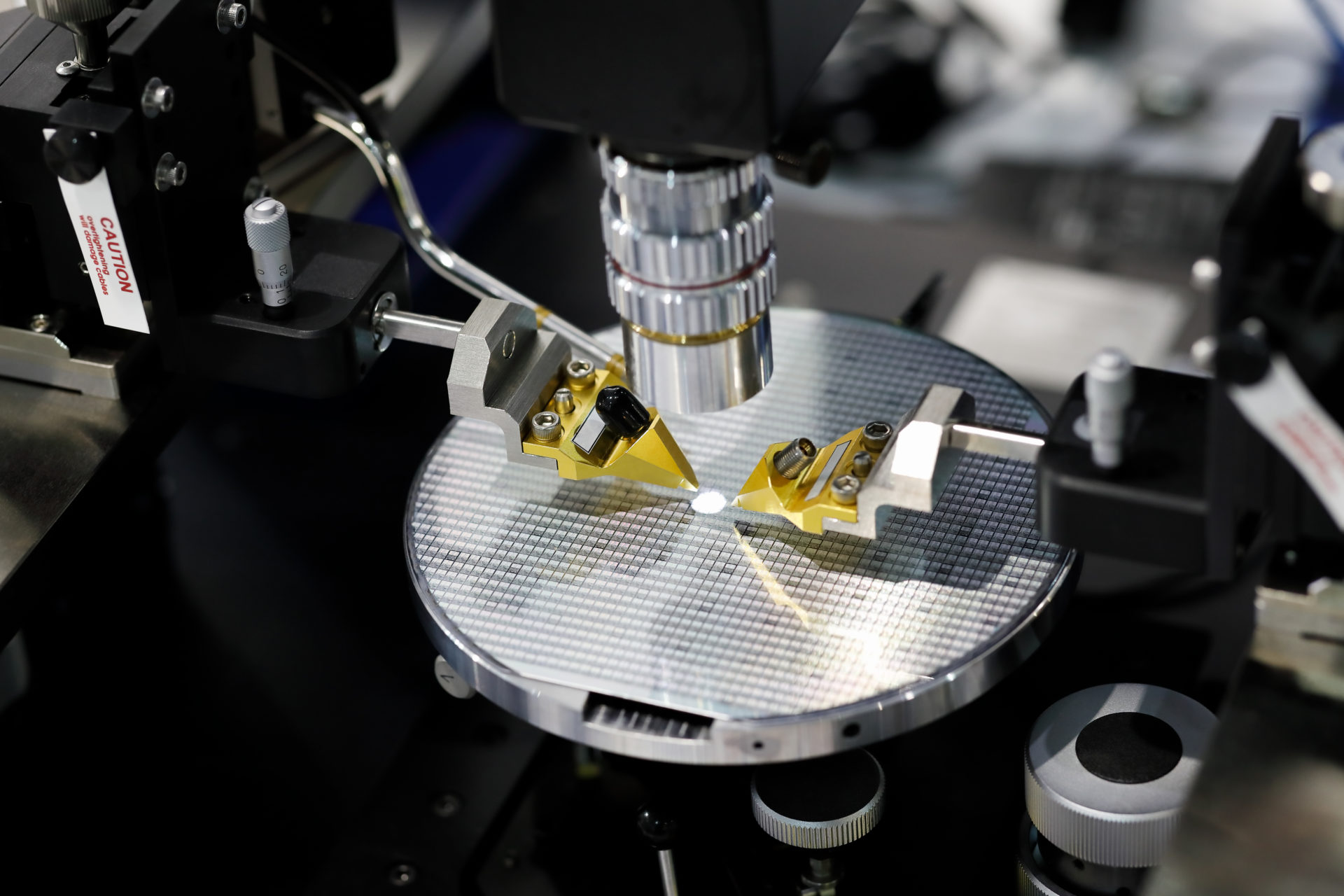
7 Best Semiconductor Inspection Equipment [Hardware & Software]

Semiconductor Manufacturing - EP-Power

57 Advance Packaging Semiconductor Images, Stock Photos, 3D objects ...
Semiconductor Images – Browse 545,128 Stock Photos, Vectors, and Video ...
Semiconductor Manufacturing Equipment Market Share Worth US$ 220 ...
82,702 Semiconductor equipment Images, Stock Photos & Vectors ...

Telangana awaits MeitY approval for three semiconductor projects ...
Construction Considerations for Semiconductor Manufacturing - Therma
82,702 Semiconductor equipment Images, Stock Photos & Vectors ...

Semiconductor Manufacturing, Fabrication, & Processing – MISUMI is your ...
